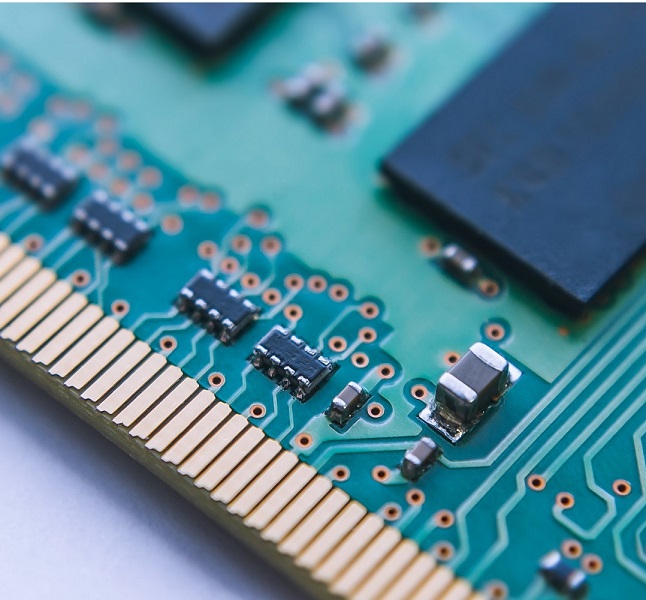
Dediprog NuProg-E2 Universal ProgrammerProduct no.: NuProg-E2NuProg-E2 is an universal engineering programmer. Widely supports most IC types on the market, UFS, eMMC, MCU, CPLD, FPGA, SPI NOR, SPI NAND, Parallel NOR, Parallel NAND and EEPROM, etc. |
ProgMaster-U4 Universal Gang Programmer(4 Sites)Product no.: ProgMaster-U4ProgMaster-U4 is a universal high-speed gear programmer with 4 programming points that supports all IC families on the market. can be shipped within 5-10 days |
Dediprog Starprog-U Universal Engineering ProgrammerProduct no.: StarProg-UStarProg-U is an engineering universal IC programmer which supports a variety of IC on the market. |
Dediprog NuProgPlus-U16 Universal Gang ProgrammerProduct no.: NuProgPlus-U16USB3.1 powerful universal programmer, support EEPROM, Flash, MCU, eMMC, UFS, PCI-E SSD and CANbus devices. can be shipped within 5-10 days |
Dediprog ProgMaster-U8 Universal Gang ProgrammerProduct no.: ProgMaster-U8ProgMaster-U8 is a high-speed gear programmer that supports all IC families on the market and has 8 programming points. can be shipped within 5-10 days |
StarProg-A Universal On Board (ICP/ISP) ProgrammerProduct no.: StarProg-AThe StarProg-A from Dediprog supports MCU, CPLD, SPI NOR Flash, SPI NAND Flash and EEPROM On Board Programming (ICP / ISP). It is optimized for the integration of automated machines and can easily be used in development and mass production.
|
Plus Vat for enduser and companies located in Germany
Complex Programmable Logic Devices (CPLD) are programmable logic circuits defined in digital technology. They are the technological successors of the Programmable Array Logic (PAL) and their structure is simpler than that of the significantly more complex Field Programmable Gate Arrays (FPGAs). However, the programming is identical.
A field programmable gate array (FPGA), also called a programmable logic gate, is an integrated circuit of digital technology, in which a logic circuit can be loaded.
The classic programming of ICs or memories differs from the "programming" of FPGAs, which is actually the creation of the circuit structure of an FPGA. This is formulated using a hardware description language (VDHL / Verilog) and translated into a configuration file using logic synthesis, which specifies how the physical elements in the FPGA should be interconnected.
There are suitable solutions for creating and simulating FPGA designs, e.g. Active HDL or Rivera Pro. In addition to graphical input (block and FSM), Active HDL also includes a text editor and the powerful ALDEC simulation environment, which supports all common languages for HDL development. In addition, prototyping boards are used for the development.
The logic switches and memories in most FPGAs are realized by SRAM memory cells, which are loaded appropriately during the boot process. This configuration data or link rules are usually loaded from a special Flash ROM module. A microcontroller can also be used. Most FPGAs therefore offer several modes for this configuration process (serial, parallel, master / slave). Since the SRAM cells lose their content when the supply voltage is switched off, an SRAM-based FPGA must be reconfigured each time it is switched on. Such an FPGA therefore takes a few milliseconds to a few seconds before it is fully operational. FPGAs with non-volatile memory are based on EEPROM, flash memory.
With the programmers we offer, it is possible to program all common FPGAs and CPLDs on the market.